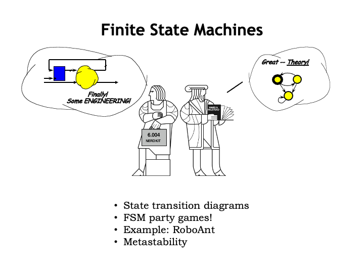
Finite State Machines
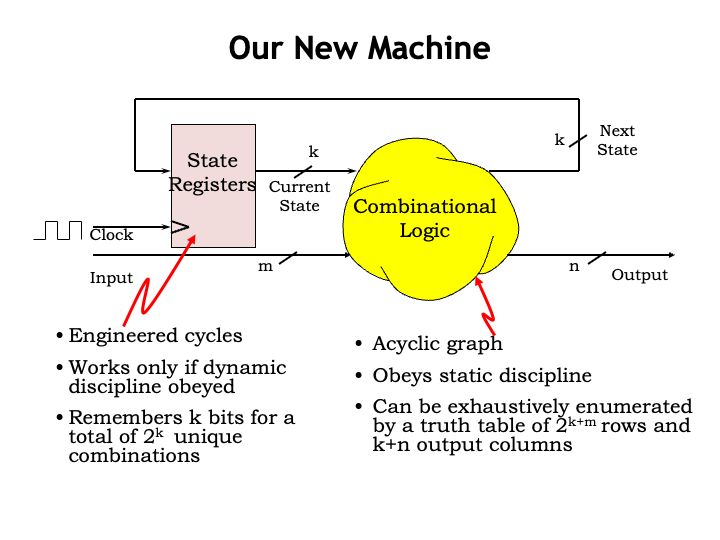
In the last lecture we developed sequential logic, which contains both combinational logic and memory components.
The combinational logic cloud is an acyclic graph of components that obeys the static discipline. The static discipline guarantees if we supply valid and stable digital inputs, then we will get valid and stable digital outputs by some specified interval after the last input transition. Thereʼs also a functional specification that tells us the output values for every possible combination of input values. In this diagram, there are k+m inputs and k+n outputs, so the truth table for the combinational logic will have $2^{k+m}$ rows and k+n output columns.
The job of the state registers is to remember the current state of the sequential logic. The state is encoded as some number k of bits, which will allow us to represent $2^k$ unique states. Recall that the state is used to capture, in some appropriate way, the relevant history of the input sequence. To the extent that previous input values influence the operation of the sequential logic, that happens through the stored state bits. Typically the LOAD input of the state registers is triggered by the rising edge of a periodic clock signal, which updates the stored state with the new state calculated by the combinational logic.
As designers we have several tasks: first we must decide what output sequences need to be generated in response to the expected input sequences. A particular input may, in fact, generate a long sequence of output values. Or the output may remain unchanged while the input sequence is processed, step-by-step, where the FSM is remembering the relevant information by updating its internal state. Then we have to develop the functional specification for the logic so it calculates the correct output and next state values. Finally, we need to come up with an actual circuit diagram for sequential logic system.
All the tasks are pretty interesting, so letʼs get started!
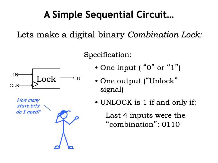
As an example sequential system, letʼs make a combination lock. The lock has a 1-bit input signal, where the user enters the combination as a sequence of bits. Thereʼs one output signal, UNLOCK, which is 1 if and only if the correct combination has been entered. In this example, we want to assert UNLOCK, i.e., set UNLOCK to 1, when the last four input values are the sequence 0-1-1-0.
Mr. Blue is asking a good question: how many state bits do we need? Do we have to remember the last four input bits? In which case, weʼd need four state bits. Or can we remember less information and still do our job? Aha! We donʼt need the complete history of the last four inputs, we only need to know if the most recent entries represent some part of a partially-entered correct combination. In other words if the input sequence doesnʼt represent a correct combination, we donʼt need to keep track of exactly how itʼs incorrect, we only need to know that is incorrect.
With that observation in mind, letʼs figure out how to represent the desired behavior of our digital system.
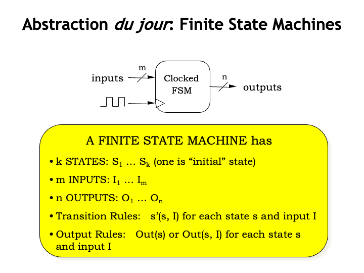
We can characterize the behavior of a sequential system using a new abstraction called a finite state machine, or FSM for short. The goal of the FSM abstraction is to describe the input/output behavior of the sequential logic, independent of its actual implementation.
A finite state machine has a periodic CLOCK input. A rising clock edge will trigger the transition from the current state to the next state. The FSM has a some fixed number of states, with a particular state designated as the initial or starting state when the FSM is first turned on. One of the interesting challenges in designing an FSM is to determine the required number of states since thereʼs often a tradeoff between the number of state bits and the complexity of the internal combinational logic required to compute the next state and outputs.
There are some number of inputs, used to convey all the external information necessary for the FSM to do its job. Again, there are interesting design tradeoffs. Suppose the FSM required 100 bits of input. Should we have 100 inputs and deliver the information all at once? Or should we have a single input and deliver the information as a 100-cycle sequence? In many real world situations where the sequential logic is much faster than whatever physical process weʼre trying to control, weʼll often see the use of bit-serial inputs where the information arrives as a sequence, one bit at a time. That will allow us to use much less signaling hardware, at the cost of the time required to transmit the information sequentially.
The FSM has some number outputs to convey the results of the sequential logicʼs computations. The comments before about serial vs. parallel inputs applies equally to choosing how information should be encoded on the outputs.
There are a set of transition rules, specifying how the next state S-prime is determined from the current state S and the inputs I. The specification must be complete, enumerating S-prime for every possible combination of S and I.
And, finally, thereʼs the specification for how the output values should be determined. The FSM design is often a bit simpler if the outputs are strictly a function of the current state S, but, in general, the outputs can be a function of both S and the current inputs.
Now that we have our abstraction in place, letʼs see how to use it to design our combinational lock.
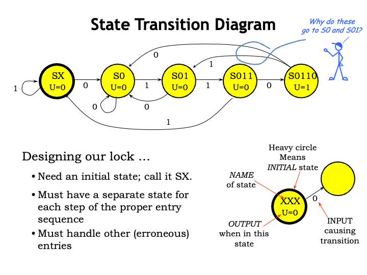
Weʼll describe the operation of the FSM for our combination lock using a state transition diagram. Initially, the FSM has received no bits of the combination, a state weʼll call SX. In the state transition diagram, states are represented as circles, each labeled for now with a symbolic name chosen to remind us of what history it represents. For this FSM, the unlock output U will be a function of the current state, so weʼll indicate the value of U inside the circle. Since in state SX we know nothing about past input bits, the lock should stay locked and so U = 0. Weʼll indicate the initial state with a wide border on the circle.
Weʼll use the successive states to remember what weʼve seen so far of the input combination. So if the FSM is in state SX and it receives a 0 input, it should transition to state S0 to remind us that weʼve seen the first bit of the combination of 0-1-1-0. We use arrows to indicate transitions between states and each arrow has a label telling us when that transition should occur. So this particular arrow is telling us that when the FSM is in state SX and the next input is a 0, the FSM should transition to state S0. Transitions are triggered by the rising edge of the FSMʼs clock input.
Letʼs add the states for the remainder of the specified combination. The rightmost state, S0110, represents the point at which the FSM has detected the specified sequence of inputs, so the unlock signal is 1 in this state. Looking at the state transition diagram, we see that if the FSM starts in state SX, the input sequence 0-1-1-0 will leave the FSM in state S0110.
So far, so good. What should the FSM do if an input bit is not the next bit in the combination? For example, if the FSM is in state SX and the input bit is a 1, it still has not received any correct combination bits, so the next state is SX again. Here are the appropriate non-combination transitions for the other states. Note that an incorrect combination entry doesnʼt necessarily take the FSM to state SX. For example, if the FSM is in state S0110, the last four input bits have been 0-1-1-0. If the next input is a 1, then the last four inputs bits are now 1-1-0-1, which wonʼt lead to an open lock. But the last two bits might be the first two bits of a valid combination sequence and so the FSM transitions to S01, indicating that a sequence of 0-1 has been entered over the last two bits.

Weʼve been working with an FSM where the outputs are function of the current state, called a Moore machine. Here the outputs are written inside the state circle.
If the outputs are a function of both the current state and the current inputs, itʼs called a Mealy machine. Since the transitions are also a function of the current state and current inputs, weʼll label each transition with appropriate output values using a slash to separate input values from output values. So, looking at the state transition diagram on the right, suppose the FSM is in state S3. If the input is a 0, look for the arrow leaving S3 labeled “0/”. The value after the slash tells us the output value, in this case 1. If the input had been a 1, the output value would be 0.
There are some simple rules we can use to check that a state transition diagram is well formed. The transitions from a particular state must be mutually exclusive, i.e., for a each state, there canʼt be more than one transition with the same input label. This makes sense: if the FSM is to operate consistently there canʼt be any ambiguity about the next state for a given current state and input. By consistently we mean that the FSM should make the same transitions if itʼs restarted at the same starting state and given the same input sequences.
Moreover, the transitions leaving each state should be collectively exhaustive, i.e., there should a transition specified for each possible input value. If we wish the FSM to stay in itʼs current state for that particular input value, we need to show a transition from the current state back to itself.
With these rules there will be exactly one transition selected for every combination of current state and input value.
FSM Implementation
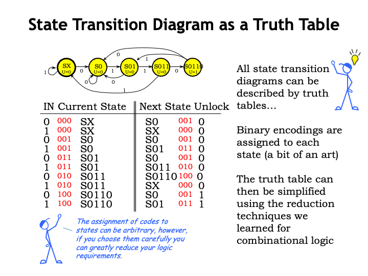
All the information in a state transition diagram can be represented in tabular form as a truth table. The rows of the truth table list all the possible combinations of current state and inputs. And the output columns of the truth table tell us the next state and output value associated with each row.
If we substitute binary values for the symbolic state names, we end up with a truth table just like the ones we saw in Lecture 4. If we have K states in our state transition diagram weʼll need $\log_2 K$ state bits, rounded up to the next integer since we donʼt have fractional bits! In our example, we have a 5-state FSM, so weʼll need 3 state bits.
We can assign the state encodings in any convenient way, e.g., 000 for the first state, 001 for the second state, and so on. But the choice of state encodings can have a big effect on the logic needed to implement the truth table. Itʼs actually fun to figure out the state encoding that produces the simplest possible logic.
With a truth table in hand, we can use the techniques from Lecture 4 to design logic circuits that implement the combinational logic for the FSM. Of course, we can take the easy way out and simply use a read-only memory to do the job!
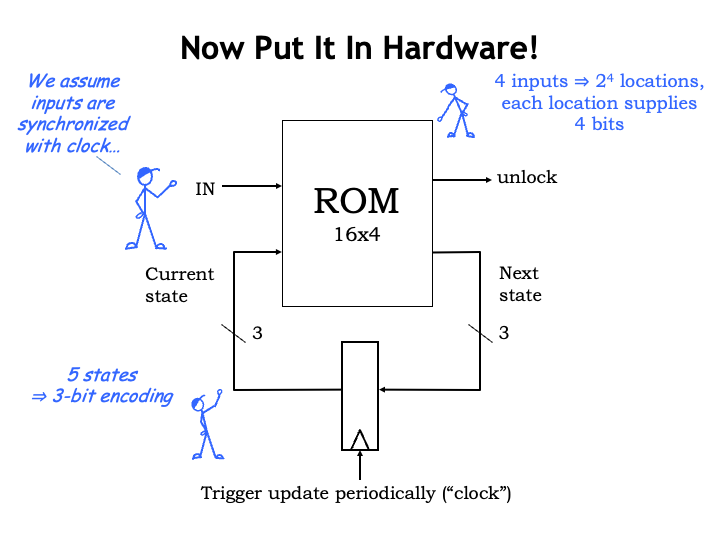
In this circuit, a read-only memory is used to compute the next state and outputs from the current state and inputs. Weʼre encoding the 5 states of the FSM using a 3-bit binary value, so we have a 3-bit state register. The rectangle with the edge-triggered input is schematic shorthand for a multi-bit register. If a wire in the diagram represents a multi-bit signal, we use a little slash across the wire with a number to indicate how many bits are in the signal. In this example, both current_state and next_state are 3-bit signals.
The read-only memory has a total of 4 input signals — 3 for the current state and 1 for the input value — so the read-only memory has $2^4= 16$ locations, which correspond to the 16 rows in the truth table. Each location in the ROM supplies the output values for a particular row of the truth table. Since we have 4 output signals — 3 for the next state and 1 for the output value — each location supplies 4 bits of information. Memories are often annotated with their number of locations and the number of bits in each location. So our memory is a 16-by-4 ROM: 16 locations of 4-bits each.
Of course, in order for the state registers to work correctly, we need to ensure that the dynamic discipline is obeyed. We can use the timing analysis techniques described at the end of Lecture 5 to check that this is so. For now, weʼll assume that the timing of transitions on the inputs are properly synchronized with the rising edges of the clock.
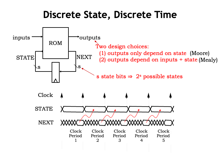
So now we have the FSM abstraction to use when designing the functionality of a sequential logic system, and a general-purpose circuit implementation of the FSM using a ROM and a multi-bit state register. Recapping our design choices: the output bits can be strictly a function of the current state (the FSM would then be called a Moore machine), or they can be a function of both the current state and current inputs, in which case the FSM is called a Mealy machine. We can choose the number of state bits — S state bits will give us the ability to encode $2^S$ possible states. Note that each extra state bit DOUBLES the number of locations in the ROM! So when using ROMs to implement the necessary logic, weʼre very interested in minimizing the number of state bits.
The waveforms for our circuitry are pretty straightforward. The rising edge of the clock triggers a transition in the state register outputs. The ROM then does its thing, calculating the next state, which becomes valid at some point in the clock cycle. This is the value that gets loaded into the state registers at the next rising clock edge. This process repeats over-and-over as the FSM follows the state transitions dictated by the state transition diagram.
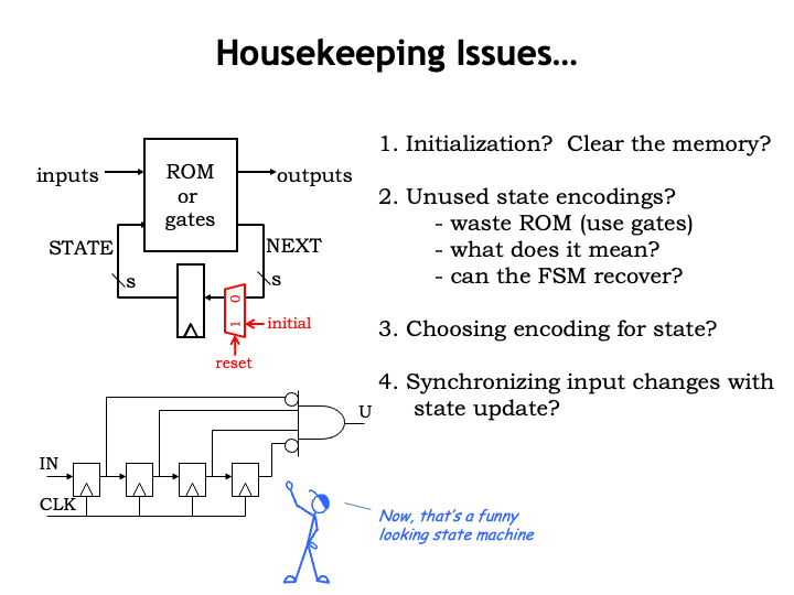
There are a few housekeeping details that need our attention.
On start-up we need some way to set the initial contents of the state register to the correct encoding for the initial state. Many designs use a RESET signal thatʼs set to 1 to force some initial state and then set to 0 to start execution. We could adopt that approach here, using the RESET signal to select an initial value to be loaded into the state register.
In our example, we used a 3-bit state encoding which would allow us to implement an FSM with up to $2^3 = 8$ states. Weʼre only using 5 of these encodings, which means there are locations in the ROM weʼll never access. If thatʼs a concern, we can always use logic gates to implement the necessary combinational logic instead of ROMs. Suppose the state register somehow got loaded with one of the unused encodings? Well, that would be like being in a state thatʼs not listed in our state transition diagram. One way to defend against this problem is design the ROM contents so that unused states always point to the initial state. In theory the problem should never arise, but with this fix at least it wonʼt lead to unknown behavior.
We mentioned earlier the interesting problem of finding a state encoding that minimized the combinational logic. There are computer-aided design tools to help do this as part of the larger problem of finding minimal logic implementations for Boolean functions. Mr. Blue is showing us another approach to building the state register for the combination lock: use a shift register to capture the last four input bits, then simply look at the recorded history to determine if it matches the combinations. No fancy next state logic here!
Finally, we still have to address the problem of ensuring that input transitions donʼt violate the dynamic discipline for the state register. Weʼll get to this in the last section of this lecture.
Letʼs think a bit more about the FSM abstraction.
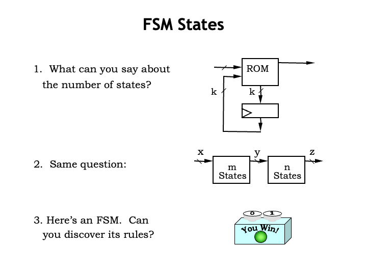
If we see an FSM that uses K state bits, what can we say about the number of states in its state transition diagram? Well, we know the FSM can have at most $2^K$ states, since thatʼs the number of unique combinations of K bits.
Suppose we connect two FSMs in series, with the outputs of the first FSM serving as the inputs to the second. This larger system is also an FSM — how many states does it have? Well, if we donʼt know the details of either of the component FSMs, the upper bound on the number of states for the larger system is M*N. This is because it may be possible for the first FSM to be in any of its M states while the second FSM is any of its N states. Note that the answer doesnʼt depend on X or Y, the number of input signals to each of the component FSMs. Wider inputs just mean that there are longer labels on the transitions in the state transition diagram, but doesnʼt tell us anything about the number of internal states.
Finally, hereʼs a question thatʼs a bit trickier than it seems. I give you an FSM with two inputs labeled 0 and 1, and one output implemented as a light. Then I ask you to discover its state transition diagram. Can you do it? Just to be a bit more concrete, you experiment for an hour pushing the buttons in a variety of sequences. Each time you push the 0 button the light turns off if it was on. And when you push the 1 button the light turns on if it was off, otherwise nothing seems to happen. What state transition diagram could we draw based on our experiments?

Consider the following two state transition diagrams. The top diagram describes the behavior we observed in our experiments: pushing 0 turns the light off, pushing 1 turns the light on.
The second diagram appears to do the same thing unless you happened to push the 1 button 4 times in a row!
If we donʼt have an upper bound on the number of states in the FSM, we can never be sure that weʼve explored all of its possible behaviors.
But if we do have an upper bound, say, K, on the number of states and we reset the FSM to its initial state, we can discover its behavior. This is because in a K-state FSM every reachable state can reached in less than K transitions, starting from the initial state. So if we try all the possible K-step input sequences one after the other starting each trial at the initial state, weʼll be guaranteed to have visited every state in the machine.
Our answer is also complicated by the observation that FSMs with different number of states may be equivalent.
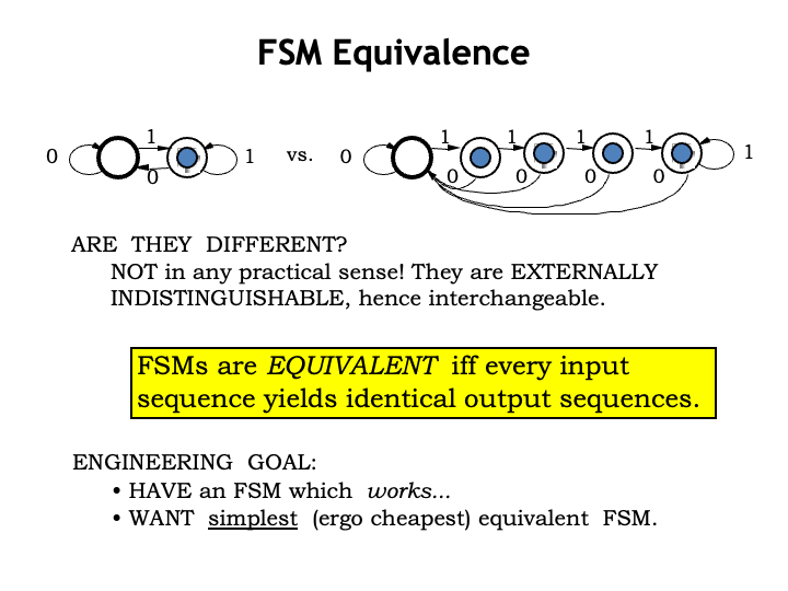
Here are two FSMs, one with 2 states, one with 5 states. Are they different? Well, not in any practical sense. Since the FSMs are externally indistinguishable, we can use them interchangeably. We say that two FSMs are equivalent if and only if every input sequence yields identical output sequences from both FSMs.
So as engineers, if we have an FSM we would like to find the the simplest (and hence the least expensive) equivalent FSM. Weʼll talk about how to find smaller equivalent FSMs in the context of our next example.
FSM Example: Roboant
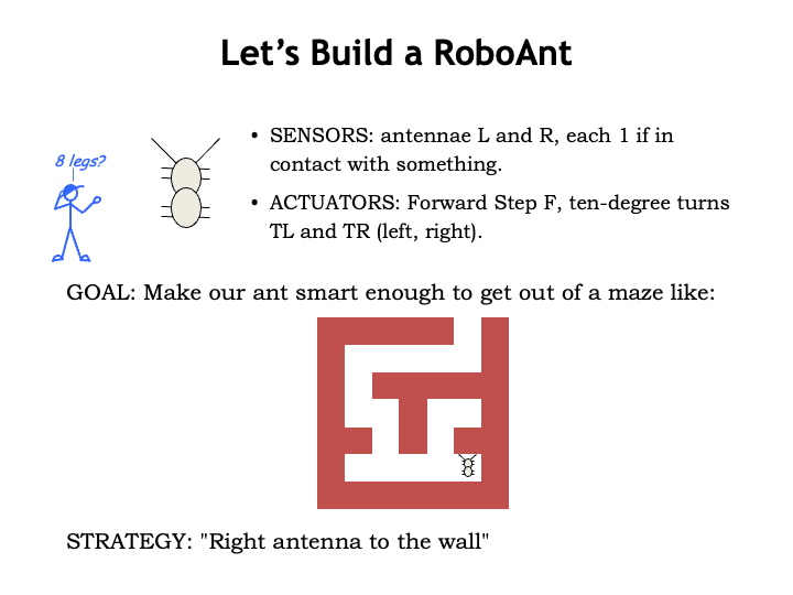
Surprise! Weʼve just been given a robotic ant that has an FSM for its brain. The inputs to the FSM come from the antʼs two antennae, labeled L and R. An antenna input is 1 if the antenna is touching something, otherwise its 0. The outputs of the FSM control the antʼs motion. We can make it step forward by setting the F output to 1, and turn left or right by asserting the TL or TR outputs respectively. If the ant tries to both turn and step forward, the turn happens first. Note that the ant can turn when its antenna are touching something, but it canʼt move forward. Weʼve been challenged to design an ant brain that will let it find its way out of a simple maze like the one shown here.
We remember reading that if the maze doesnʼt have any unconnected walls (i.e.,no islands), we can escape using the right-hand rule where we put our right hand on the wall and walk so that our hand stays on the wall.
Letʼs try to implement this strategy.
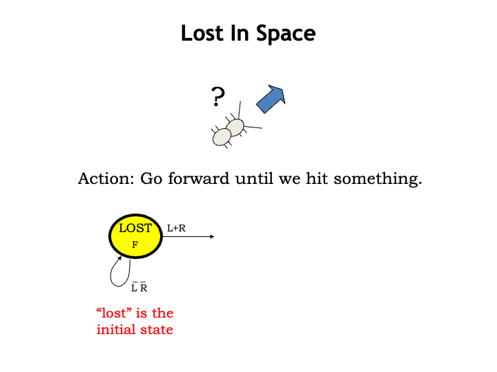
Weʼll assume that initially our ant is lost in space. The only sensible strategy to walk forward until we find a maze wall. So our initial state, labeled LOST, asserts the F output, causing the ant to move forward until at least one of the antennae touches something, i.e., at least one of the L or R inputs is a 1.
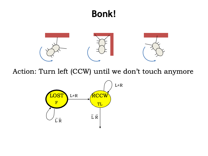
So now the ant finds itself in one of these three situations. To implement the right-hand rule, the ant should turn left (counterclockwise) until itʼs antennae have just cleared the wall. To do this, weʼll add a rotate-counterclockwise state, which asserts the turn-left output until both L and R are 0.
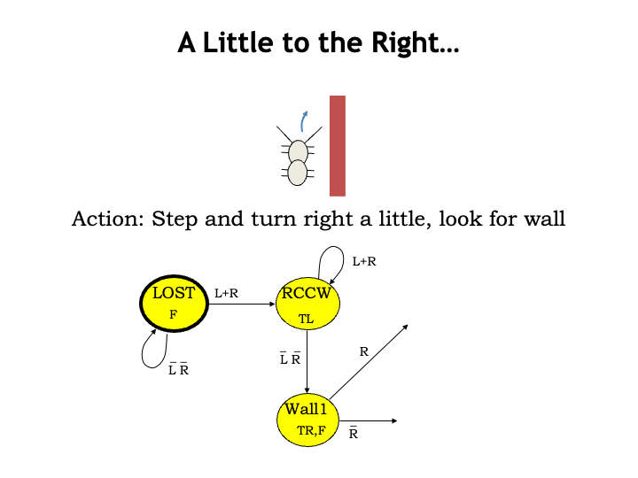
Now the ant is standing with a wall to its right and we can start the process of following the wall with its right antenna. So we have the ant step forward and right, assuming that it will immediately touch the wall again. The WALL1 state asserts both the turn-right and forward outputs, then checks the right antenna to see what to do next.
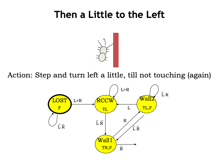
If the right antenna does touch, as expected, the ant turns left to free the antenna and then steps forward. The WALL2 state asserts both the turn-left and forward outputs, then checks the antennae. If the right antenna is still touching, it needs to continue turning. If the left antenna touches, itʼs run into a corner and needs to reorient itself so the new wall is on its right, the situation we dealt with the rotate-counterclockwise state. Finally, if both antennae are free, the ant should be in the state of the previous slide: standing parallel to the wall, so we return the WALL1 state.
Our expectation is that the FSM will alternate between the WALL1 and WALL2 states as the ant moves along the wall. If it reaches an inside corner, it rotates to put the new wall on its right and keeps going. What happens when it reaches an outside corner?
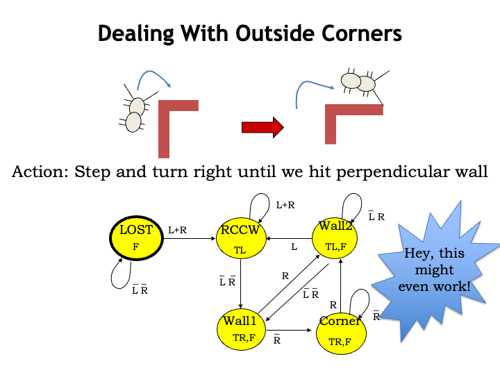
When the ant is in the WALL1 state, it moves forward and turns right, then checks its right antenna, expecting the find the wall its traveling along. But if its an outside corner, thereʼs no wall to touch! The correct strategy in this case is to keep turning right and stepping forward until the right antenna touches the wall thatʼs around the corner. The CORNER state implements this strategy, transitioning to the WALL2 state when the ant reaches the wall again.
Hey, this might even work!
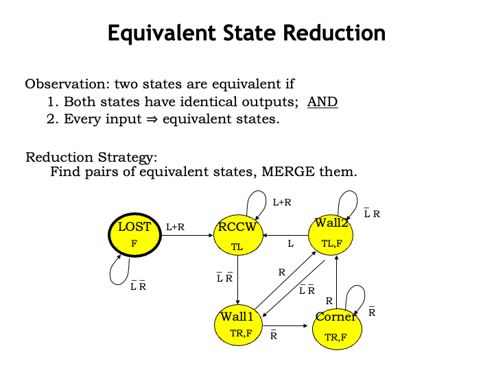
Earlier we talked about about finding equivalent FSMs with fewer states. Now weʼll develop an approach for finding such FSMs by looking for two states that that can be merged into a single state without changing the behavior of the FSM in any externally distinguishable manner.
Two states are equivalent if they meet the following two criteria. First, the states must have identical outputs. This makes sense: the outputs are visible to the outside, so if their values differed between the two states, that difference would clearly be externally distinguishable!
Second, for each combination of input values, the two states transition to equivalent states.
Our strategy for deriving an equivalent machine with fewer states will be to start with our original FSM, find pairs of equivalent states and merge those states. Weʼll keep repeating the process until we canʼt find any more equivalent states.
Letʼs try this on our ant FSM. First we need to find a pair of states that have the same outputs. As it turns out, thereʼs only one such pair: WALL1 and CORNER, both of which assert the turn-right and forward outputs.
Okay, so letʼs assume that WALL1 and CORNER are equivalent and ask if they transition to equivalent states for each applicable combination of input values. For these two states, all the transitions depend only on the value of the R input, so we just have to check two cases. If R is 0, both states transition to CORNER. If R is 1, both states transition to WALL2.
So both equivalence criteria are satisfied and we can conclude that the WALL1 and CORNER states are equivalent and can be merged.

This gives us the four-state FSM shown here, where weʼve called the single merged state WALL1. This smaller, equivalent FSM behaves exactly as the previous 5-state FSM. The implementation of the 5-state machine requires 3 state bits; the implementation of the 4-state machine only requires 2 state bits. Reducing the number of state bits by 1 is huge since it reduces the size of the required ROM by half!
Just as we were able to achieve considerable hardware savings by minimizing Boolean equations, we can do the same in sequential logic by merging equivalent states.
Roboant customers are looking forward to the price cut!
The simulation below uses the 4-state FSM we just finished to show Roboant in action. Click RUN to get things started!
After each step (state transition) the FSM display highlights the line was just completed and the Maze display shows the updated position and rotation of the ant.
If you want to give Roboant a real workout, click on HAMPTON to select the famous hedge maze from Hampton Court in England. Note that you can resize the simulation window by clicking and dragging its lower right-hand corner.
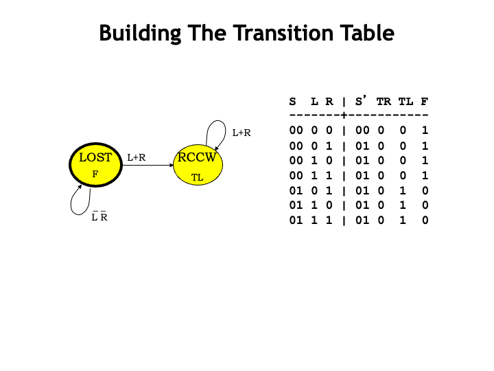
Letʼs look at what weʼd need to do if we wanted to implement the FSM using logic gates instead a ROM for the combinational logic. First we have to build the truth table, entering all the transitions in the state transition diagram. Weʼll start with the LOST state. So if the FSM is in this state, the F output should be 1. If both antenna inputs are 0, the next state is also LOST. Assigning the LOST state the encoding 00, weʼve captured this information in the first row of the table.
If either antenna is touching, the FSM should transition from LOST to the rotate-counterclockwise state. Weʼve given this an encoding of 01. There are three combinations of L and R values that match this transition, so weʼve added three rows to the truth table. This takes care of all the transitions from the LOST state.
Now we can tackle the transitions from the rotate-counterclockwise state. If either antenna is touching, the next state is again rotate-counterclockwise. So weʼve identified the matching values for the inputs and added the appropriate three rows to the transition table.
We can continue in a similar manner to encode the transitions one-by-one.
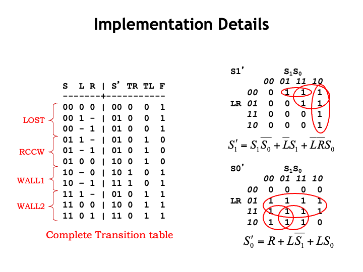
Hereʼs the final table, where weʼve used donʼt cares to reduce the number of rows for presentation. Next we want to come up with Boolean equations for each of the outputs of the combinational logic, i.e., the two next-state bits and the three motion-control outputs.
Here are the Karnaugh maps for the two next-state bits. Using our K-map skills from Lecture 4, weʼll find a cover of the prime implicants for S1-prime and write down the corresponding product terms in a minimal sum-of-products equation. And then do the same for the other next-state bit.
We can follow a similar process to derive minimal sum-of-products expressions for the motion-control outputs.
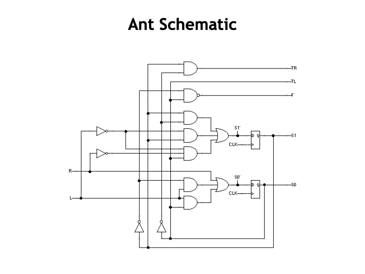
Implementing each sum-of-products in a straight-forward fashion with AND and OR gates, we get the following schematic for the ant brain. Pretty neat! Who knew that maze following behavior could be implemented with a couple of D registers and a handful of logic gates?
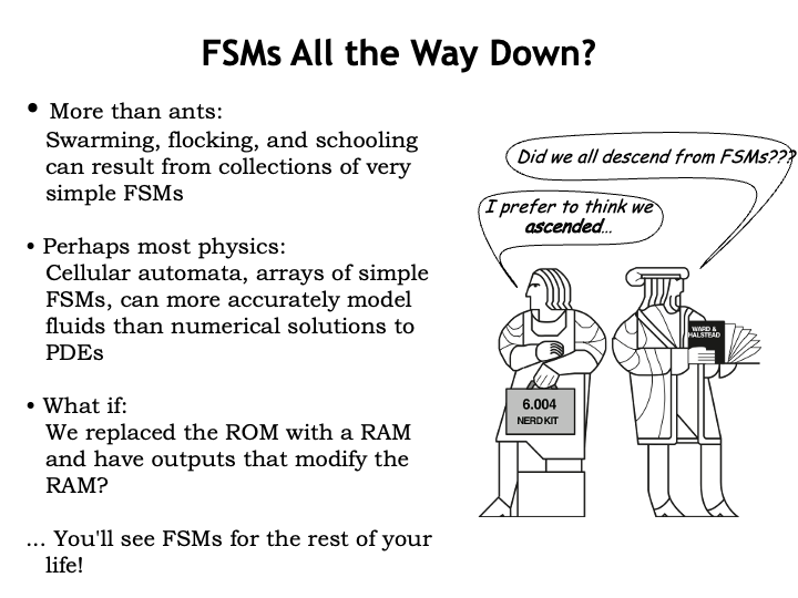
There are many complex behaviors that can be created with surprisingly simple FSMs. Early on, the computer graphics folks learned that group behaviors like swarming, flocking and schooling can be modeled by equipping each participant with a simple FSM. So next time you see the massive battle scene from the Lord of the Rings movie, think of many FSMs running in parallel!
Physical behaviors that arise from simple interactions between component molecules can sometimes be more easily modeled using cellular automata — arrays of communicating FSMS — than by trying to solve the partial differential equations that model the constraints on the moleculesʼ behavior.
And hereʼs an idea: what if we allowed the FSM to modify its own transition table? Hmm. Maybe thatʼs a plausible model for evolution!
FSMs are everywhere! Youʼll see FSMs for the rest of your life...
Synchronization and Metastability
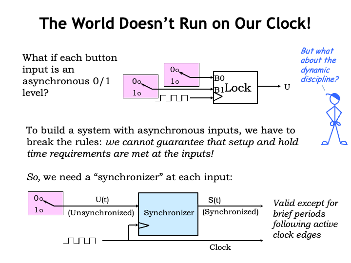
Okay, itʼs finally time to investigate issues caused by asynchronous inputs to a sequential logic circuit. By asynchronous we mean that the timing of transitions on the input is completely independent of the timing of the sequential logic clock. This situation arises when the inputs arrive from the outside world where the timing of events is not under our control.
As we saw at the end the lecture on “Sequential Logic”, to ensure reliable operation of the state registers, inputs to a sequential logic system have to obey setup and hold time constraints relative to the rising edge of the system clock. Clearly if the input can change at anytime, it can change at time that would violate the setup and hold times.
Maybe we can come up with a synchronizer circuit that takes an unsynchronized input signal and produces a synchronized signal that only changes shortly after the rising edge of the clock. Weʼd use a synchronizer on each asynchronous input and solve our timing problems that way.
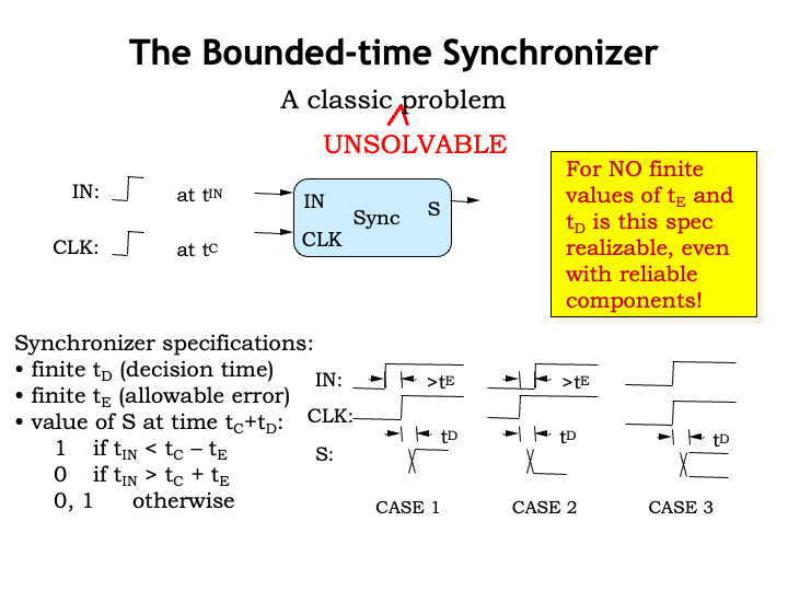
Hereʼs a detailed specification for our synchronizer.
The synchronizer has two inputs, IN and CLK, which have transitions at time $t_{\textrm{IN}}$ and $t_{\textrm{C}}$ respectively.
If INʼs transition happens sufficiently before Cʼs transition, we want the synchronizer to output a 1 within some bounded time $t_{\textrm{D}}$ after CLKʼs transition.
And if CLKʼs transition happens sufficient before INʼs transition, we want the synchronizer to output a 0 within time $t_{\textrm{D}}$ after CLKʼs transition.
Finally, if the two transitions are closer together than some specified interval $t_{\textrm{E}}$, the synchronizer can output either a 0 or a 1 within time $t_{\textrm{D}}$ of CLKʼs transition. Either answer is fine so long as itʼs a stable digital 0 or digital 1 by the specified deadline.
This turns out to be an unsolvable problem! For no finite values of $t_{\textrm{E}}$ and $t_{\textrm{D}}$ can we build a synchronizer thatʼs guaranteed to meet this specification even when using components that are 100% reliable.
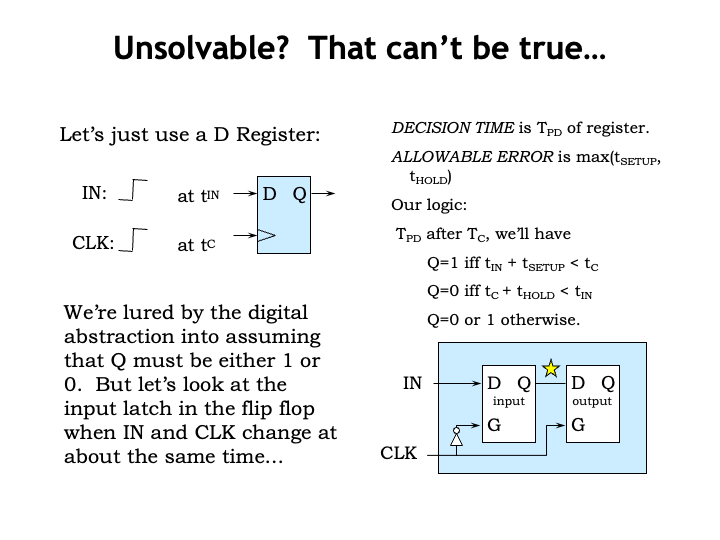
But canʼt we just use a D register to solve the problem? Weʼll connect IN to the registerʼs data input and connect CLK to the registerʼs clock input. Weʼll set the decision time $t_{\textrm{D}}$ to the propagation delay of the register and the allowable error interval to the larger of the registerʼs setup and hold times.
Our theory is that if the rising edge of IN occurs at least $t_{\textrm{SETUP}}$ before the rising edge of CLK, the register is guaranteed to output a 1. And if IN transitions more than $t_{\textrm{HOLD}}$ after the rising edge of CLK, the register is guaranteed to output a 0. So far, so good. If IN transitions during the setup and hold times with respect to the rising edge on CLK, we know weʼve violated the dynamic discipline and we canʼt tell whether the register will store a 0 or a 1. But in this case, our specification lets us produce either answer, so weʼre good to go, right?
Sadly, weʼre not good to go. Weʼre lured by the digital abstraction into assuming that even if we violate the dynamic discipline that Q must be either 1 or 0 after the propagation delay. But that isnʼt a valid assumption as weʼll see when we look more carefully at the operation of the registerʼs master latch when B and C change at about the same time.
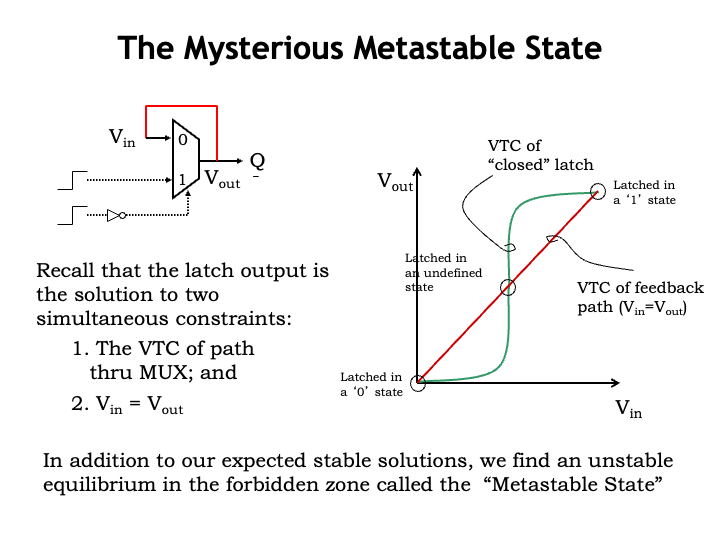
Recall that the master latch is really just a lenient MUX that can be configured as a bi-stable storage element using a positive feedback loop. When the latch is in memory mode, itʼs essentially a two-gate cyclic circuit whose behavior has two constraints: the voltage transfer characteristic of the two-gate circuit, shown in green on the graph, and that $V_{\textrm{IN}}$ equals $t_{\textrm{OUT}}$, a constraint thatʼs shown in red on the graph.
These two curves intersect at three points. Our concern is the middle point of intersection. If IN and CLK change at the same time, the voltage on Q may be in transition at the time the MUX closes and enables the positive feedback loop. So the initial voltage in the feedback loop may happen to be at or very near the voltage of the middle intersection point.
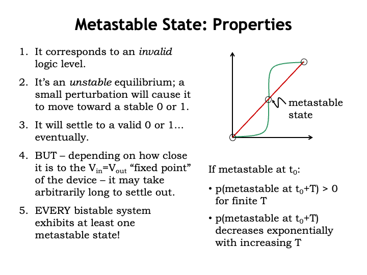
When Q is at the metastable voltage, the storage loop is in an unstable equilibrium called the metastable state. In theory the system could balance at this point forever, but a small change in the voltages in the loop will move the system away from the metastable equilibrium point and set it irrevocably in motion towards the stable equilibrium points. Hereʼs the issue we face: we canʼt bound the amount of time the system will spend in the metastable state.
Hereʼs what we know about the metastable state.
Itʼs in the forbidden zone of the digital signaling specifications and so corresponds to an invalid logic level. Violating the dynamic discipline means that our register is no longer guaranteed to produce a digital output in bounded time.
A persistent invalid logic level can wreak both logical and electrical havoc in our sequential logic circuit. Since combinational logic gates with invalid inputs have unpredictable outputs, an invalid signal may corrupt the state and output values in our sequential system.
At the electrical level, if an input to a CMOS gate is at the metastable voltage, both PFET and NFET switches controlled by that input would be conducting, so weʼd have a path between $V_{\textrm{DD}}$ and GND, causing a spike in the systemʼs power dissipation.
Itʼs an unstable equilibrium and will eventually be resolved by a transition to one of the two stable equilibrium points. You can see from the graph that the metastable voltage is in the high-gain region of the VTC, so a small change in $V_{\textrm{IN}}$ results in a large change in $t_{\textrm{OUT}}$, and once away from the metastable point the loop voltage will move towards 0 or $V_{\textrm{DD}}$.
The time it takes for the system to evolve to a stable equilibrium is related to how close Qʼs voltage was to the metastable point when the positive feedback loop was enabled. The closer Qʼs initial voltage is to the metastable voltage, the longer it will take for the system to resolve the metastability. But since thereʼs no lower bound on how close Q is to the metastable voltage, thereʼs no upper bound on the time it will take for resolution. In other words, if you specify a bound, e.g., $t_{\textrm{D}}$, on the time available for resolution, thereʼs a range of initial Q voltages that wonʼt be resolved within that time.
If the system goes metastable at some point in time, then thereʼs a non-zero probability that the system will still be metastable after some interval T, for any finite choice of T.
The good news is that the probability of being metastable at the end of the interval decreases exponentially with increasing T.
Note that every bistable system has at least one metastable state. So metastability is the price we pay for building storage elements from positive feedback loops.
If youʼd like to read a more thorough discussion of synchronizers and related problems and learn about the mathematics behind the exponential probabilities, please see Lecture 10 of the Course Notes.
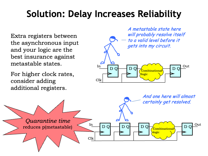
Our approach to dealing with asynchronous inputs is to put the potentially metastable value coming out of our D-register synchronizer into quarantine by adding a second register hooked to the output of the first register.
If a transition on the input violates the dynamic discipline and causes the first register to go metastable, itʼs not immediately an issue since the metastable value is stopped from entering the system by the second register. In fact, during the first half of the clock cycle, the master latch in the second register is closed, so the metastable value is being completely ignored.
Itʼs only at the next clock edge, an entire clock period later, that the second D register will need a valid and stable input. Thereʼs still some probability that the first register will be metastable after an entire clock period, but we can make that probability as low as we wish by choosing a sufficiently long clock period. In other words, the output of the second register, which provides the signal used by the internal combinational logic, will be stable and valid with a probability of our choosing. Validity is not 100% guaranteed, but the failure times are measured in years or decades, so itʼs not an issue in practice. Without the second register, the system might see a metastability failure every handful of hours — the exact failure rate depends on the transition frequencies and gains in the circuit.
What happens if our clock period is short but we want a long quarantine time? We can use multiple quarantine registers in series — itʼs the total delay between when the first register goes metastable and when the synchronized input is used by the internal logic that determines the failure probability.
The bottom line: we can use synchronizing registers to quarantine potentially metastable signals for some period of time. Since the probability of still being metastable decreases exponentially with the quarantine time, we can reduce the failure probability to any desired level. Not a 100% guaranteed, but close enough that metastability is not a practical issue if we use our quarantine strategy.